
The transistor: the switch inside everything
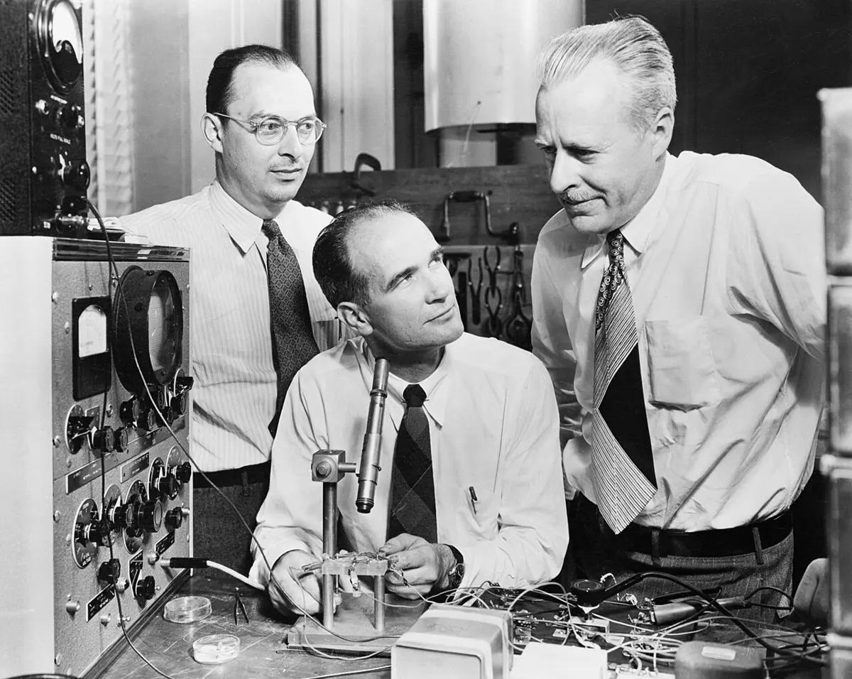
Nobel Prize in Physics, 1956: William Shockley, John Bardeen, and Walter Brattain
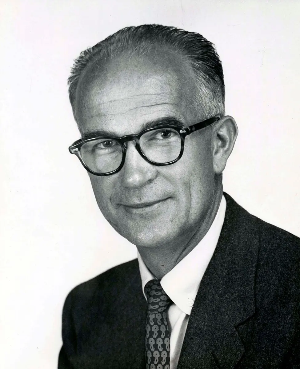
William Shockley
1910–1989, born in Britain
He led the team, and within weeks of his colleagues’ invention he had worked out a better transistor on his own. In 1956 he founded the first company to make silicon transistors in what became Silicon Valley.
Photo: Nobel foundation, Public domain
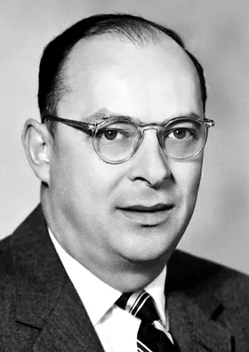
John Bardeen
1908–1991, born in the USA
A quiet theorist who explained why the first attempts had failed. In 1972 he won the Nobel Prize in Physics a second time, the only person ever to win it twice.
Photo: Nobel foundation, Public domain
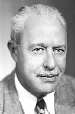
Walter Brattain
1902–1987, born in China
An experimenter with clever hands, who grew up on a cattle ranch in the north-west of the United States and built the first transistor himself.
Photo: Nobel foundation, Public domain
Your phone is a pocket full of switches. Its main chip holds well over ten billion of them, each one far too small to see, each turning on and off billions of times every second. They are called transistors.
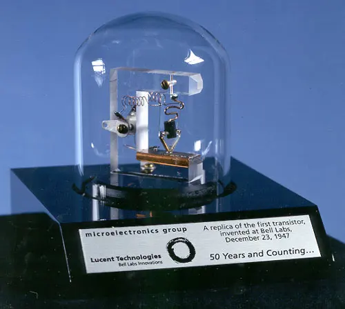
The first transistor, made in 1947, was the size of a thumbnail and held together with a paper clip. In 1956 the three men who invented it, William Shockley, John Bardeen and Walter Brattain, won the Nobel Prize in Physics.
The problem: hot, fragile glass bulbs
Before the transistor, electronics ran on vacuum tubes, also called valves. A vacuum tube is a glass bulb with the air pumped out. Inside, a filament is heated until it glows, like the wire of an old light bulb, and it gives off electrons. A small voltage on a wire mesh inside the bulb controls how many electrons reach a metal plate at the other end. So a small, weak signal can control a big current. That is called amplifying: making a signal bigger. Vacuum tubes could also be used as switches, turning a current on and off.
Radios, televisions, telephone exchanges and the first computers were all built from vacuum tubes. But they had serious faults:
- They were big: each was about the size of a thumb or bigger.
- They used a lot of power and got hot, because the filament had to glow all the time Grade 9: Heating effect of electric current.
- They burnt out, like light bulbs, and had to be replaced.
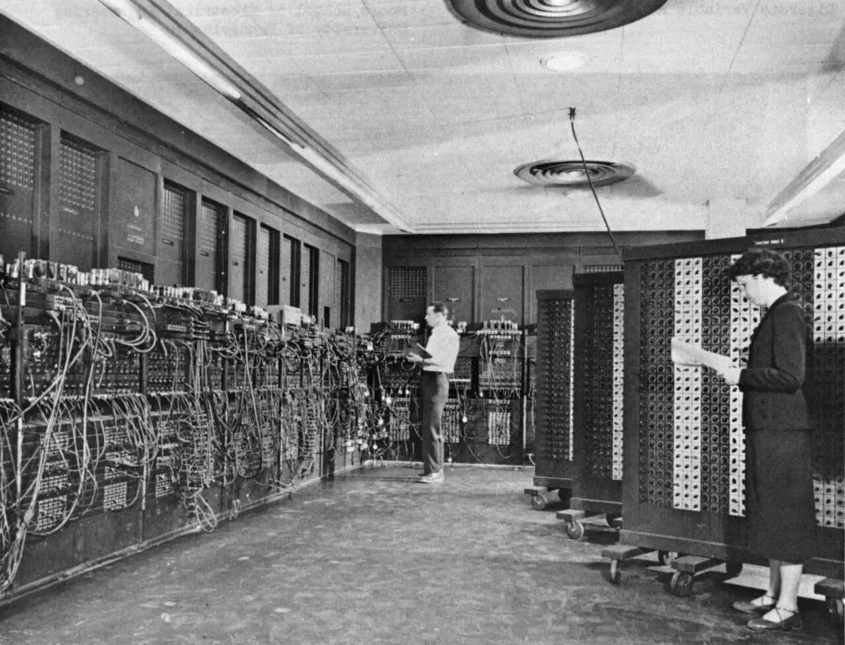
One of the first electronic computers, ENIAC, finished in the United States at the end of 1945, had about 17,500 vacuum tubes. It filled a large room, weighed about 30 tonnes and used about 150 kW of electricity. Tubes burnt out so often that keeping it running was a job in itself.
The American telephone company AT&T, whose network was full of vacuum-tube amplifiers and mechanical switches, wanted something better. In 1945 its research laboratory, Bell Telephone Laboratories (Bell Labs) in Murray Hill, New Jersey, set up a team to find something better, made from solid material instead of glowing glass. Its leader was William Shockley.
How a semiconductor works
The team chose to work with semiconductors.
Some materials, the conductors such as copper, let electricity flow easily, because they have plenty of free electrons. Others, the insulators such as glass and plastic, hardly let it flow at all, because their electrons are held tightly Grade 8: Conductors and insulators. Semiconductors are in between. The two most important are silicon and germanium, metalloids in the same group as carbon in the periodic table Grade 10: Metalloids.
Their great trick is that you can choose how well they conduct. Each silicon or germanium atom has four outer electrons, and in the crystal all four are used to hold on to the atoms around it Grade 9: Valence electrons. So a pure crystal has very few free electrons. But replace a few atoms in every hundred thousand with another element, and it changes completely. This is called doping.
- Add a little phosphorus, which has five outer electrons: each phosphorus atom has one electron left over, free to move. This is n-type material (n for negative).
- Add a little boron, which has only three outer electrons: each boron atom leaves a gap where an electron is missing, called a hole. Electrons nearby can jump into the hole, so the hole moves around like a positive charge. This is p-type material (p for positive).
Small crystals of silicon and germanium were already used in the Second World War, in diodes for radar sets, which let current through one way only. The work on radar taught people how to make these crystals very pure, and that made the transistor possible.
Pure silicon hardly conducts electricity. A few phosphorus atoms are added. Why does it now conduct much better?
Pick an answer to see why.
Why it was hard
Shockley’s first idea, in 1945, was simple. Lay a thin layer of semiconductor under a metal plate. Put a voltage on the plate, and its electric push should pull extra electrons into the semiconductor, so that it conducts better. A small voltage on the plate would then control a big current: an amplifier with no hot filament.
It didn’t work. The current hardly changed at all.
John Bardeen worked out why. The electrons pulled towards the plate got stuck at the surface of the semiconductor, trapped in surface states, a thin skin of trapped charge. The trapped electrons shielded the inside of the crystal from the plate’s push, the way a crowd standing at a gate stops anyone else from getting through. To make a transistor, the team first had to understand surfaces, something nobody knew much about.
What they did, step by step
Bardeen and Brattain: two gold points
Walter Brattain was the experimenter, who had studied semiconductor surfaces at Bell Labs since 1929. John Bardeen, a theorist, joined the team in late 1945. They worked side by side: Bardeen suggested experiments, Brattain built and ran them, and they discussed the results every day.
- 1946–1947, the surface. Following Bardeen’s idea, Brattain studied what happens at the surface of silicon and germanium. In November 1947 they found that a drop of liquid on the surface could break the trapped layer, and the current began to respond.
- December 1947, the wedge. Brattain wrapped a strip of gold foil round a small plastic triangle and carefully cut through the foil at its tip with a razor blade. That gave two gold contacts only about 0.05 mm apart, closer than the width of a hair. A spring, made from a bent paper clip, pressed the tip onto a slab of germanium.
- 16 December 1947, it works. A small current fed into one gold contact controlled a much bigger current through the other. The signal came out up to about 100 times stronger. This was the first point-contact transistor.
- 23 December 1947, the demonstration. They showed it to the laboratory’s managers by amplifying speech: a voice spoken into the circuit came out louder in the headphones.
Shockley: the junction transistor
Shockley was proud of the team’s success, but upset that the breakthrough was not his own. Working alone, over the following weeks, partly in a hotel room in Chicago where he was attending a meeting, he thought out a better design.
- 23 January 1948, the idea. Instead of delicate gold points pressed on a surface, Shockley’s transistor was a solid sandwich of three layers of doped semiconductor, n-p-n, with a very thin middle layer. A small current into the middle layer controls a large current through the whole sandwich.
- 30 June 1948, the announcement. Bell Labs showed the transistor to the press in New York. The name was suggested by an engineer at Bell Labs, John Pierce, from “transfer resistor”. Few newspapers paid much attention.
- 1949–1951, the theory and the real thing. Shockley published his theory of the junction transistor in 1949. By 1951 Bell Labs could make junction transistors that worked. They were tough, reliable and could be made in factories. Within a few years they were in hearing aids and pocket radios.
What was the main advantage of the transistor over the vacuum tube?
Pick an answer to see why.
How it works now: switches on a chip
Today almost all transistors are of a third kind, the one Shockley tried first in 1945: the field-effect transistor. In 1959 two engineers at Bell Labs, Mohamed Atalla and Dawon Kahng, finally made it work, by growing a very thin layer of glass-like silicon dioxide on the silicon. The layer cleans up the surface, so that electrons are no longer trapped there. This kind of transistor is called a MOSFET.
It works like a tap. A strip of silicon has two connections, the source and the drain. Above the strip, separated by the thin insulating layer, is a third connection, the gate.
- Gate off: no current can flow between source and drain. The switch is off: in a computer, a 0.
- Gate on: a small positive voltage on the gate pulls electrons up to the surface of the silicon, just under the gate. They form a thin channel joining source and drain, and current flows. The switch is on: a 1.
Almost no current flows into the gate itself, because of the insulator. So turning the switch on and off costs very little energy.
Computers count in binary, with only the digits 0 and 1 Grade 10: Binary numbers. Each transistor holds or passes one 0 or 1. Connected together in their billions, transistors add numbers, store photos, and run apps.
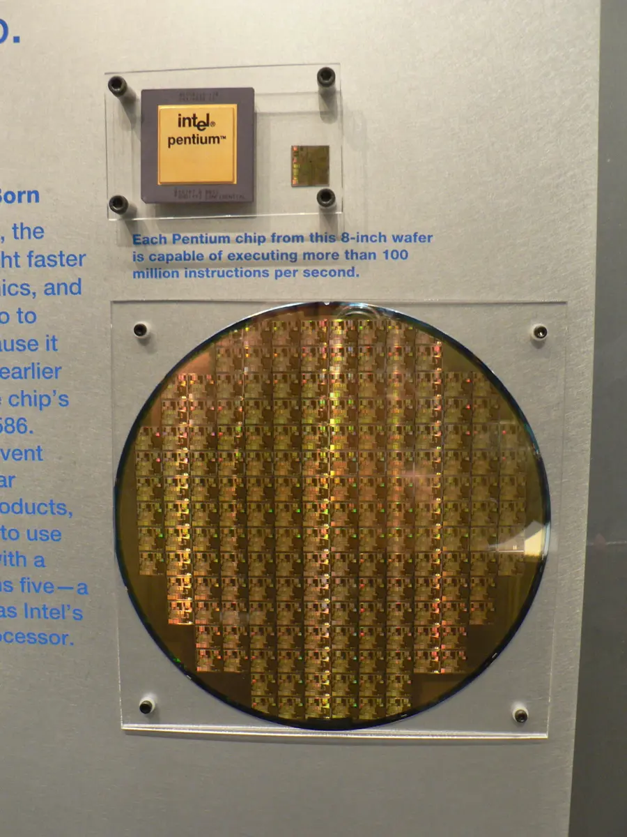
The other great step was to make many transistors together, on one piece of silicon, already joined up. This is the integrated circuit, or chip, made in 1958 and 1959 by Jack Kilby and Robert Noyce (Kilby won the Nobel Prize in Physics in 2000). Ever since, engineers have found ways to make transistors smaller, so that more fit on a chip.
In your life today
- Your phone. A phone’s main chip has well over ten billion transistors, and its memory many more.
- Everything with a battery. Calculators, digital watches, TV remotes, the electronic meter on your house and the controller of a solar lamp all run on transistors. So do phone chargers and the controls of electric buses and cars.
- The most numerous thing ever made. By one estimate, made in 2018 by the Computer History Museum in California, about 13 sextillion transistors (13 followed by 21 zeros) had been made since 1947, more than any other thing people have ever made.
What came next
- Silicon Valley. In 1956 Shockley moved to California and set up his own company to make silicon transistors. He was a difficult boss, and in 1957 eight of his best scientists left to start their own company, Fairchild Semiconductor. From it came Intel and many others. The area south of San Francisco became known as Silicon Valley.
- Bardeen’s second prize. Bardeen moved to the University of Illinois and, with two younger physicists, explained superconductivity, why some metals lose all electrical resistance when very cold. They won the Nobel Prize in Physics in 1972.
- Shockley’s later years. In later life Shockley became known less for science than for his views on race and intelligence, which scientists showed to be wrong and which are widely condemned.
- Smaller and smaller. In 1971 the smallest parts of a chip were about 10 micrometers across. Today some parts of the newest transistors are only a few nanometers, a few dozen atoms, across.
An open question: transistors cannot keep shrinking for ever, because a switch must be made of at least some atoms, and at such small sizes electrons can leak straight through a switch that is off. Engineers are now stacking transistors in layers, and trying new materials. How computers will keep getting more powerful in twenty years’ time is an open question.
In your science books
- Grade 8: conductors and insulators.
- Grade 9: electric current, the heating effect of electric current (why vacuum tubes got hot) and valence electrons, the four outer electrons of silicon.
- Grade 10: metalloids, Mendeleev’s periodic table (germanium was his eka-silicon), analog and digital signals and binary numbers.
- More Nobel Prizes built on semiconductors: the CCD camera sensor and blue LEDs.
Learn more
- The prize at nobelprize.org: The Nobel Prize in Physics 1956, with the presentation speech, which ends with the comparison to Everest.
- The three Nobel lectures: Shockley, Bardeen and Brattain.
The official reason
The prize was given “for their researches on semiconductors and their discovery of the transistor effect.”