
The chip and the tiny laser
Nobel Prize in Physics, 2000: Zhores Alferov, Herbert Kroemer, and Jack Kilby
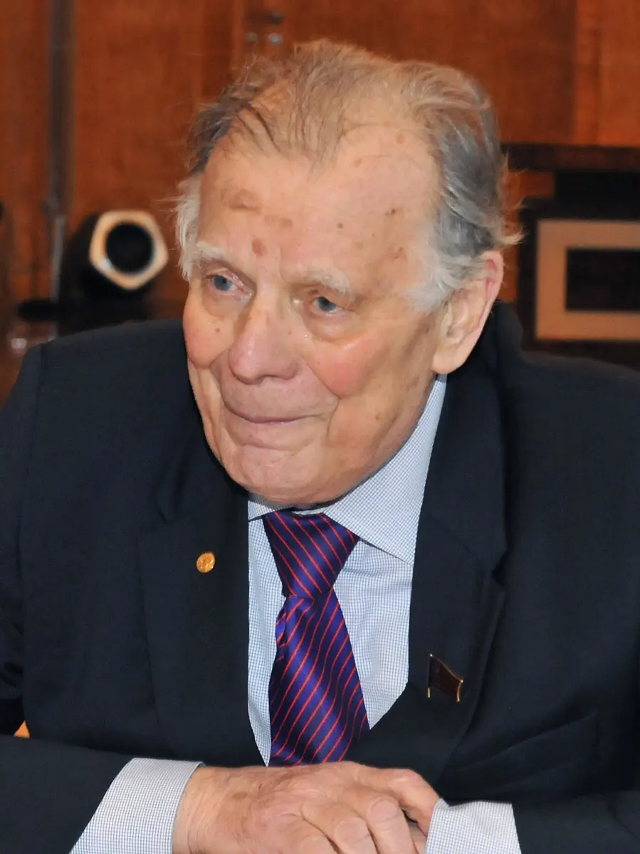
Zhores Alferov
1930–2019, born in Vitebsk (now in Belarus)
He made the layered crystals work in a Leningrad laboratory, often with less equipment than his rivals, and beat them anyway.
Photo: Press service of the President of Tatarstan, CC BY 4.0
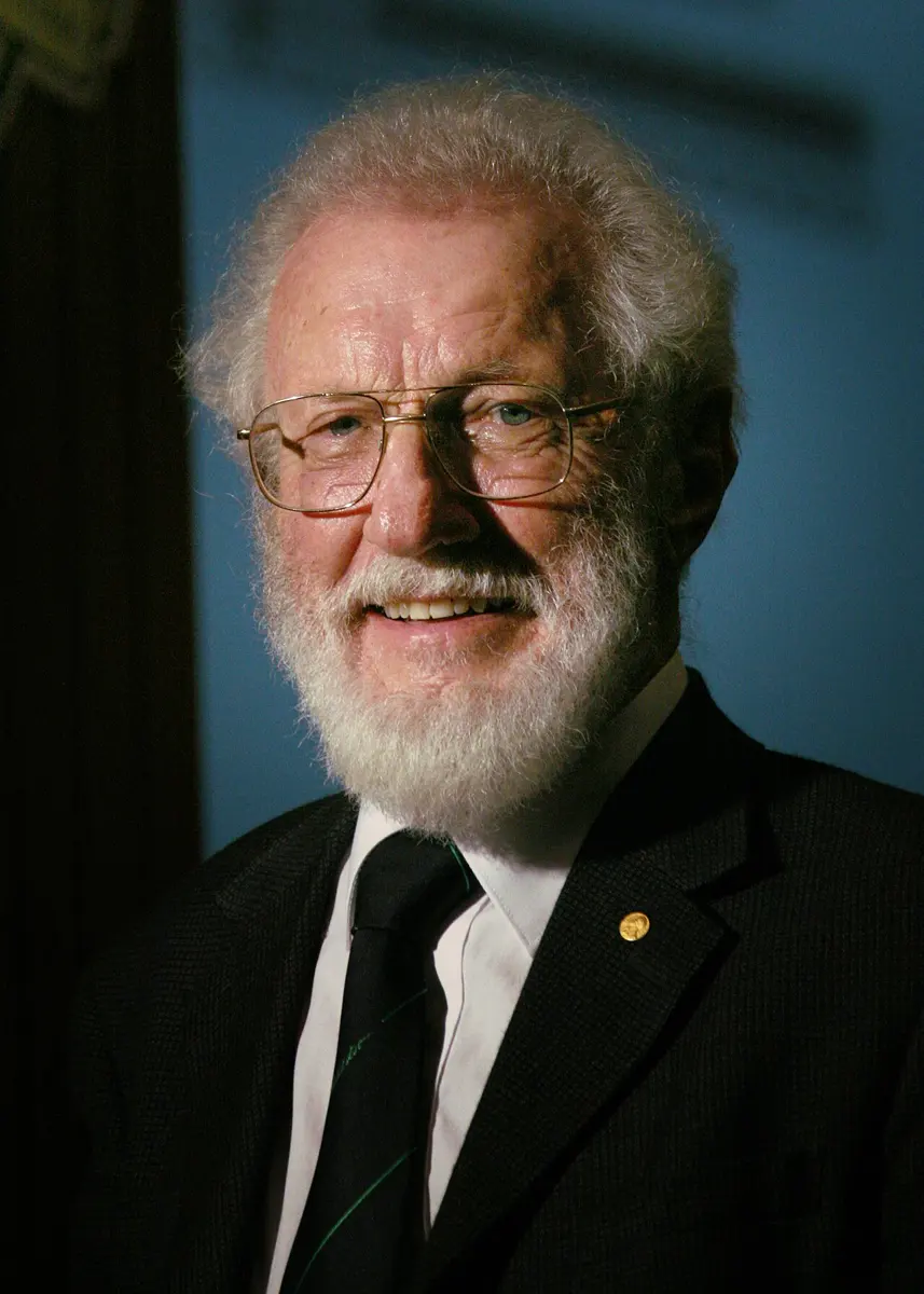
Herbert Kroemer
1928–2024, born in Weimar, Germany
A theorist who saw the idea first, and was told it could never have any use.
Photo: Javier Chagoya, Public domain
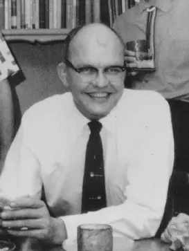
Jack Kilby
1923–2005, born in the USA
A quiet engineer from Kansas who fell in love with electronics through his father’s amateur radio.
Photo: James R. Biard, CC BY-SA 4.0
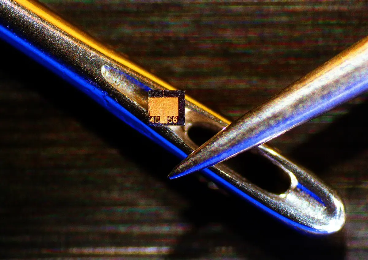
Look inside a mobile phone and you will find a few flat black chips, each smaller than a stamp. Inside each chip are billions of tiny switches, all made at the same time in one piece of silicon. And when you watch a video, it has probably traveled most of the way to you as flashes of light along a glass thread, flashes made by a laser smaller than a grain of salt.
The Nobel Prize in Physics 2000 was given for both of these: Jack Kilby, for his part in inventing the integrated circuit (the chip), and Zhores Alferov and Herbert Kroemer, for heterostructures: crystals built up in thin layers of different semiconductors, which made tiny lasers and very fast transistors possible.
The problem: too many parts, and lasers that burned out
Too many wires
In 1947 the transistor was invented: a small switch and amplifier made from a semiconductor, which replaced the hot, fragile glass valves of old radios (see the transistor). By the 1950s, transistors were small and cheap. But every circuit still needed other parts too: resistors (which hold back current), capacitors (which store a little charge) and diodes (which let current through one way only). Each part was made separately, and then all of them were joined with wires and solder, by hand.
A computer needed tens of thousands of parts, and every joint was a place where something could break. The more parts, the less reliable and the more expensive the machine. Engineers called this the tyranny of numbers: they could design circuits far bigger than anyone could build.
Lasers that only worked in the cold
A laser gives a narrow beam of light of one exact color. In 1962, scientists in the USA made the first lasers out of a tiny crystal of a semiconductor, gallium arsenide. They were wonderfully small, but they had to be cooled to about −200 °C, and they worked only in short flashes. At room temperature they needed about a hundred times more electric current, which heated them until they were damaged. A laser like that was no use in a telephone line or a music player.
How it works: semiconductors and the band gap
A semiconductor is a material that conducts electricity better than an insulator but much worse than a metal. Silicon and germanium are semiconductors; they lie between the metals and the non-metals in the periodic table, and are called metalloids Grade 10: Metalloids. Gallium arsenide, made of gallium and arsenic, is a semiconductor too.
In a semiconductor, most electrons are held in place. To set one free to move, you must give it a certain amount of energy, called the band gap. When a freed electron leaves, it also leaves a gap behind, called a hole, which can move too and behaves like a positive charge.
The band gap is different in each material, and it matters in two ways:
- It decides the color of light. When a free electron falls back into a hole, it gives up energy equal to the band gap. In a laser or an LED, that energy comes out as light (see blue LEDs). A bigger gap gives bluer light, a smaller gap redder light, or infrared light that we can’t see.
- It acts like a step. Where a material with a small band gap meets one with a big band gap, an electron or a hole in the small-gap material can’t climb into the other one. It is like a ball in a ditch.
A crystal made of layers of two different semiconductors is called a heterostructure (“hetero” means different). The meeting place of two layers is a heterojunction.
A free electron falls into a hole in a semiconductor and gives out light. What decides the color of the light?
Pick an answer to see why.
Why it was hard
For the chip, the idea itself was not new. Since the early 1950s, a few engineers had suggested making all the parts of a circuit in one block of semiconductor. But the factories of the time made each part from the material that suited it best and cost least: resistors from carbon, capacitors from metal and plastic. Making a resistor out of costly pure semiconductor sounded silly. And nobody had shown that it worked.
For the layers, the problem was the crystal itself. In a crystal, the atoms sit in a perfect, regular pattern. If you grow a layer of one material on top of another, the atoms of the two must be spaced the same, like bricks of the same size, or the joint is full of faults. Electrons and holes get caught at the faults and waste their energy as heat. For years, most scientists thought good heterojunctions could never be made, and that the idea was only a dream.
What they did, step by step
Kroemer: the idea, twice
Herbert Kroemer grew up in Weimar, Germany. In 1948, as a young physics student, he escaped from East Germany to the West on one of the empty planes flying back from the Berlin airlift.
- 1954 and 1957, a faster transistor. Early transistors were slow. Kroemer worked out that a transistor would work better and faster if one part of it was made of a semiconductor with a wider band gap than the rest. He sketched the idea in 1954 and published it in full in 1957, while working at RCA in the USA. This is the heterostructure transistor.
- 1963, a laser that could work warm. At a talk at his company, Varian, Kroemer heard experts say that a semiconductor laser could never work steadily at room temperature: the electrons and holes spread out of the thin working layer too quickly. He saw at once what to do. Put the working layer between two layers with a wider band gap, and the electrons and holes would be trapped in it. This is the double heterostructure.
- No one listened. His paper was turned down by the first journal he sent it to. And when he asked to work on the new laser, his company refused, saying it could never have any use. He moved on to other work and played no part in building it.
Alferov: making it real
Zhores Alferov was born in 1930 in Vitebsk, in what was then the Soviet Union. His elder brother, Marx, was killed in the Second World War. In 1953 Alferov joined the Ioffe Institute in Leningrad (now St Petersburg), where he helped to make the first Soviet transistors.
- 1963, the same idea. Working on his own, without knowing of Kroemer, Alferov proposed the same double-heterostructure laser and patented it.
- Finding layers that fit. For years his team searched for two semiconductors whose atoms were spaced alike. They found that aluminium gallium arsenide, in which some of the gallium atoms are replaced by aluminium, fits gallium arsenide almost perfectly, but has a wider band gap. In 1969 they grew the first clean heterostructures of these two.
- May 1970, the warm laser. Alferov’s team made a double-heterostructure laser that shone steadily, not in flashes, at room temperature. A team at Bell Labs in the USA did the same only weeks later. It was a friendly race between rival countries during the Cold War.
- Solar cells for space. The team also made heterostructure solar cells. According to Alferov, they powered Soviet satellites and, for years, the Mir space station.
Why does a double-heterostructure laser need much less current than the first semiconductor lasers?
Pick an answer to see why.
Kilby: the whole circuit in one piece
Jack Kilby was born in 1923 and grew up in Great Bend, Kansas, in the middle of the USA. When an ice storm knocked down the phone and power lines, he saw his father, who ran a small electric company, keep in touch with customers by amateur radio. That made him want to work in electronics.
- Summer 1958, a summer without a holiday. In 1958 Kilby joined Texas Instruments in Dallas. That summer, as a new employee, he had no right to a holiday yet, so he spent it at work, thinking undisturbed about the tyranny of numbers. His idea: make every part of the circuit, not only the transistors, out of the same semiconductor, in one piece.
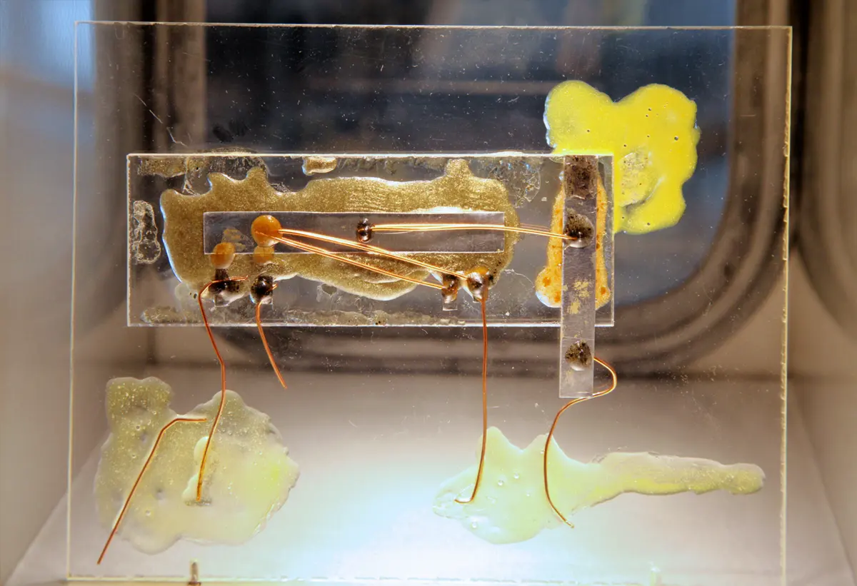
- 12 September 1958, it works. Kilby took a thin strip of germanium, about a centimeter long and less than 2 millimeters wide. In it he formed a transistor, resistors and a capacitor, and joined them with fine gold wires. He connected a battery, and a wavy signal appeared on the screen of a measuring instrument (an oscilloscope): the circuit worked. This is the birthday of the integrated circuit.
- February 1959, the patent. Texas Instruments applied for a patent on his “miniaturized electronic circuits”.
- A second inventor. A few months later, Robert Noyce, at Fairchild Semiconductor in California, worked out how to make a chip from silicon, with the connections laid flat on top instead of loose wires. This is how chips have been made ever since, so Noyce is counted as an inventor of the chip too. Noyce died in 1990, and Nobel Prizes are not given after death. Kilby said that if Noyce had been alive, he would surely have shared the prize.
How it works now
A chip
Today’s chips are made of silicon, as Noyce did it. A thin round slice of silicon, a wafer, is coated, lit through stencils and etched, over and over, in hundreds of steps. Each step makes the same pattern in every chip on the wafer at once, so billions of transistors are made together, with no soldered joints. That is why chips keep getting more powerful while staying cheap.
When Kilby made his first chip, it had one transistor. In 2000, the presenter of the prize said that the chips of the time held nearly a billion bits of memory or switches. Today a phone’s main chip has more than ten billion transistors, each far too small to see with an ordinary microscope.
A laser in a CD player or a fiber cable
The tiny laser in a CD player, a bar-code reader or an internet cable is a double heterostructure. A current is pushed through the layers; electrons and holes meet in the thin middle layer and give out light. The light bounces back and forth between the polished ends of the crystal, growing stronger, and comes out as a narrow beam.
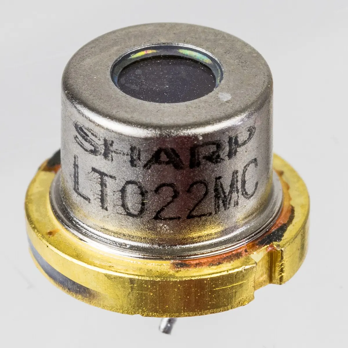
Kroemer’s fast heterostructure transistors are used where very weak, very fast signals must be picked up without drowning in noise: in mobile phone towers and in the dishes that receive signals from satellites. In 2000 they had been measured switching at 600 billion times a second, about a hundred times faster than the best ordinary transistors.
What was new about Kilby’s chip of 1958?
Pick an answer to see why.
In your life today
- Every electronic thing you use, from a phone and a computer to a digital watch, a television and a washing machine, works with integrated circuits.
- The internet. Most of the internet’s long journeys are made as flashes of laser light along optical fibers Grade 10: optical fibers in telecommunication, often from heterostructure lasers. The signals are digital: strings of 1s and 0s, each a flash or no flash Grade 10: binary numbers.
- Mobile phones. Fast heterostructure transistors are found in phones and in the towers that connect them.
- Calculators. Kilby went on to help invent the pocket calculator, one of the first things made with chips. Before it was made, a market survey found that hardly anyone wanted one.
What came next
- Smaller and smaller. The number of transistors on a chip doubled again and again, about every two years, an observation known as Moore’s law. The chip in a phone today does far more than the computers that filled whole rooms when Kilby made his first chip.
- Thinner and thinner layers. Heterostructures can be made so thin, a few atoms each, that electrons in them behave in new ways. This led to blue LEDs and lasers (see blue LEDs), to quantum dots, and to discoveries that won two more Nobel Prizes in Physics, in 1985 and 1998.
An open question: transistors are now so small that they are only a few dozen atoms across in places. They can’t shrink much further. How will chips keep getting better: by stacking layers of transistors on top of each other, by using new materials, or by computing with light instead of electricity? Engineers are trying all of these.
In your science books
- Grade 9: metals, non-metals and metalloids.
- Grade 10: metalloids, the semiconductors silicon and germanium; total internal reflection and optical fibers, which carry the light of heterostructure lasers; binary numbers, the 1s and 0s that chips work with.
- More Nobel Prizes: the transistor (1956), optical fibers and the digital camera sensor (2009) and blue LEDs (2014).
Learn more
- The prize at nobelprize.org: popular information and the presentation speech.
- The laureates’ own stories of their lives: Alferov, Kroemer and Kilby.
The official reason
The prize was given “for developing semiconductor heterostructures used in high-speed- and opto-electronics.”
The prize was given “for his part in the invention of the integrated circuit.”