
Copper carries electricity a hundred billion times better than pure silicon, and glass about a hundred billion billion times worse. Yet the three are made of atoms with much the same parts: a nucleus and electrons. Why should one solid let electrons flow and another hold them still?
The answer starts inside a single atom, whose electrons can only have certain energies, like the rungs of a ladder. Pack billions of atoms into a solid and the rungs crowd together into broad bands, separated by gaps no electron can stand in. How full the top bands are, and how wide the gap above them, decides whether a solid is a conductor, an insulator or a semiconductor. Semiconductors, with a small gap, can be changed at will, by warming them, shining light on them or adding a few atoms of another element. That is the trick behind every phone, solar panel and LED.
25.1 Energy levels
In the nuclear model of the atom (Unit 24), the electrons around a nucleus can’t have just any energy. Each electron is limited to certain energy levels, and an electron can change its energy only by jumping from one allowed level to another. Why only these levels are allowed takes the wave nature of the electron and quantum mechanics to explain (see Bohr’s staircase in Going Further). For now, accept that this is how nature works.
The levels can be drawn as horizontal lines one above the other, like a ladder with unequally spaced rungs, each line at the height of its energy: an energy level diagram. Every kind of atom has its own set of levels. An electron can move from one level to another by gaining or losing exactly the difference in energy, but it can never have an energy between two levels. So an atom can only take in or give out energy in parcels of certain definite sizes: its energy is quantized.
Hydrogen is the simplest atom: one proton with one electron bound to it by the electric force. If the atom loses its electron completely, it becomes a positive hydrogen ion. A common picture of the atom is the “planetary model”, with the electron going round the proton like the Earth round the Sun. It has weaknesses (an electron doesn’t follow a path), but it is a good introduction to energy levels.
The energy levels of the hydrogen atom are:
| Energy level, n | Energy (eV) |
|---|---|
| 1 | −13.6 |
| 2 | −3.40 |
| 3 | −1.51 |
| 4 | −0.85 |
| 5 | −0.54 |
| ∞ | 0 |
They follow one rule, : level 2 is eV, level 3 is eV.
Energies are negative because the zero is chosen with the electron free and at rest, far from the proton; a bound electron has less energy than that. An electron in the ground state of hydrogen, level 1, has exactly −13.6 eV, so 13.6 eV is needed to free it: hydrogen’s ionization energy. An atom with an electron in a level above the ground state is excited: an electron in level 2 is in the first excited state, one in level 3 in the second excited state, and so on.
The levels are discrete: an electron in a hydrogen atom can’t have −5.92 eV or −10.21 eV, or any other value between −13.6 eV and −3.40 eV. It must have one of the values in the table.
An electron in a hydrogen atom is in the second excited state. How much energy is needed to free it from the atom?
Pick an answer to see why.
25.2 Band theory
A single atom has sharp, separate energy levels. What happens to them when many atoms are packed together into a solid?
When two identical atoms are far apart, each has the same set of levels. Bring them close, and the electron waves of the two atoms overlap: each level splits into two levels, slightly apart. Bring together three atoms and each level becomes three; a grain of silicon has about 10²⁰ atoms, so each level becomes 10²⁰ levels, so close together that they form a continuous band of allowed energies, shared by all the atoms of the solid. Between the bands are gaps, ranges of energy where there are no allowed levels at all: the forbidden bands.
The valence band is the highest band that contains electrons at absolute zero; it holds the electrons of the bonds between the atoms. The band above it is the conduction band. Electrons in the conduction band are free to move through the solid and carry a current. The gap between the top of the valence band and the bottom of the conduction band is the forbidden energy gap, or band gap, .
For a current to flow, electrons must be able to gain a little energy from the electric field, which means moving into empty levels just above their own. In a full band there are no empty levels to move into, so its electrons can’t carry a current, however many there are.
Conductors. In a metal, the highest band containing electrons is only partly filled, or two bands overlap. Either way there are plenty of empty levels of slightly higher energy, so when a potential difference is applied, electrons can speed up and gain energy: a current flows easily.
Insulators. In a good insulator, the valence band is completely full and the conduction band is empty, with a wide band gap between them, typically 5 to 10 eV (diamond 5.5 eV, glass about 9 eV). At room temperature (300 K) the average kinetic energy of the particles, , is only about 0.04 eV:
So almost no electron can gain the 5 eV or more needed to cross the gap. When a potential difference is applied, there are no free levels the electrons can reach, and no current flows.
Semiconductors. A pure (or intrinsic) semiconductor, such as silicon or germanium, has bands like an insulator’s, but its band gap is much smaller, about 1 eV (silicon 1.12 eV, germanium 0.67 eV at room temperature). At room temperature a few electrons gain enough thermal energy to jump the gap into the conduction band, so a very small current can flow when a voltage is applied. At higher temperatures more electrons can jump the gap, so the resistivity of a semiconductor decreases as its temperature rises.
The widget below works these numbers out from the band gap and the temperature.
Holes
That is not all there is to a semiconductor’s current. When an electron jumps to the conduction band, it leaves an empty level behind in the valence band. Such an unfilled electron state is called a hole.
When a potential difference is applied, the few electrons in the conduction band move towards the positive electrode. The valence electrons are pulled the same way, and a few of them manage to move, by jumping into holes. Each valence electron that fills a hole leaves its own hole behind, one place back. So the holes move the other way, towards the negative electrode, as if they were positive charges. A hole carries a charge of +1.6 × 10⁻¹⁹ C, equal and opposite to an electron’s.
Electrons gather towards one side of the material and holes towards the other, and both carry the current: the electrons in the conduction band, and the holes in the valence band.
Points to remember
In an intrinsic semiconductor at 0 K:
- the valence band is completely full;
- the conduction band is empty; and
- the forbidden band is about 1 eV wide.
In an intrinsic semiconductor above 0 K:
- some electrons can jump the forbidden band into the conduction band;
- the conduction band’s electrons carry current as negative charges;
- the empty states they leave behind in the valence band are called holes;
- holes act as positive charge carriers in the valence band;
- the number of electrons per unit volume in the conduction band (their number density) equals the number density of holes in the valence band, since each jump makes one of each;
- the atoms vibrate more as the temperature rises, which on its own would raise the resistance; but the increase in the number of charge carriers far outweighs that, so overall the resistance decreases as the temperature rises.
In a metal:
- the valence band overlaps the conduction band (or the top band is partly full);
- the number of charge carriers doesn’t increase with temperature, because there is no forbidden band to cross;
- the atoms vibrate more as the temperature rises and scatter the electrons more, so the resistivity increases as the temperature rises.
In an insulator:
- the valence band is full;
- the conduction band is empty;
- the forbidden band is very wide; and
- there are no free electrons (electrons in the conduction band), so it doesn’t conduct.
Why does the resistance of a pure semiconductor decrease as its temperature rises?
Pick an answer to see why.
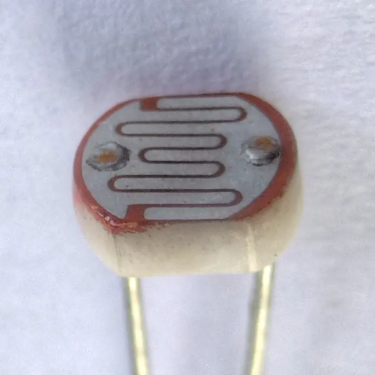
25.3 Light-dependent resistors
Thermal energy is not the only way to lift an electron from the valence band to the conduction band. A photon of light can do it too, if its energy hf is at least the band gap: the same packets of energy that knock electrons out of a metal in the photoelectric effect.
Semiconductor materials can be made with a band gap such that photons of visible light lift electrons into the conduction band. Brighter light means more photons per second, so more electrons lifted to the conduction band (and more holes left behind). So the resistance of such a material falls as the intensity of the light increases. A component made this way is a light-dependent resistor (LDR).
The usual material is cadmium sulphide, with a gap of 2.4 eV: photons of wavelength shorter than about 520 nm (green, blue and violet) can lift its electrons. A typical LDR has a resistance of about 1 MΩ in the dark and a few hundred ohms in bright sunlight.
25.4 Semiconductors
The best conductors (silver, copper and gold) have one electron in their outer shell, easily shared through the whole metal. The best semiconductors, silicon and germanium, have four. A semiconductor is a material whose electrical properties lie between those of a conductor and those of an insulator. Germanium and silicon are the elements most used; compounds such as gallium arsenide and gallium nitride are semiconductors too.
In a silicon crystal, every atom sits at the center of four neighbors and shares one of its four outer electrons with each. Each pair of shared electrons is a covalent bond, so every atom has four bonds and eight shared electrons around it: none is free to move.
The flat picture can’t show the real arrangement in space. Below is a piece of a real silicon crystal, every atom where X-ray measurements put it: pick one atom out and look at its four neighbors.
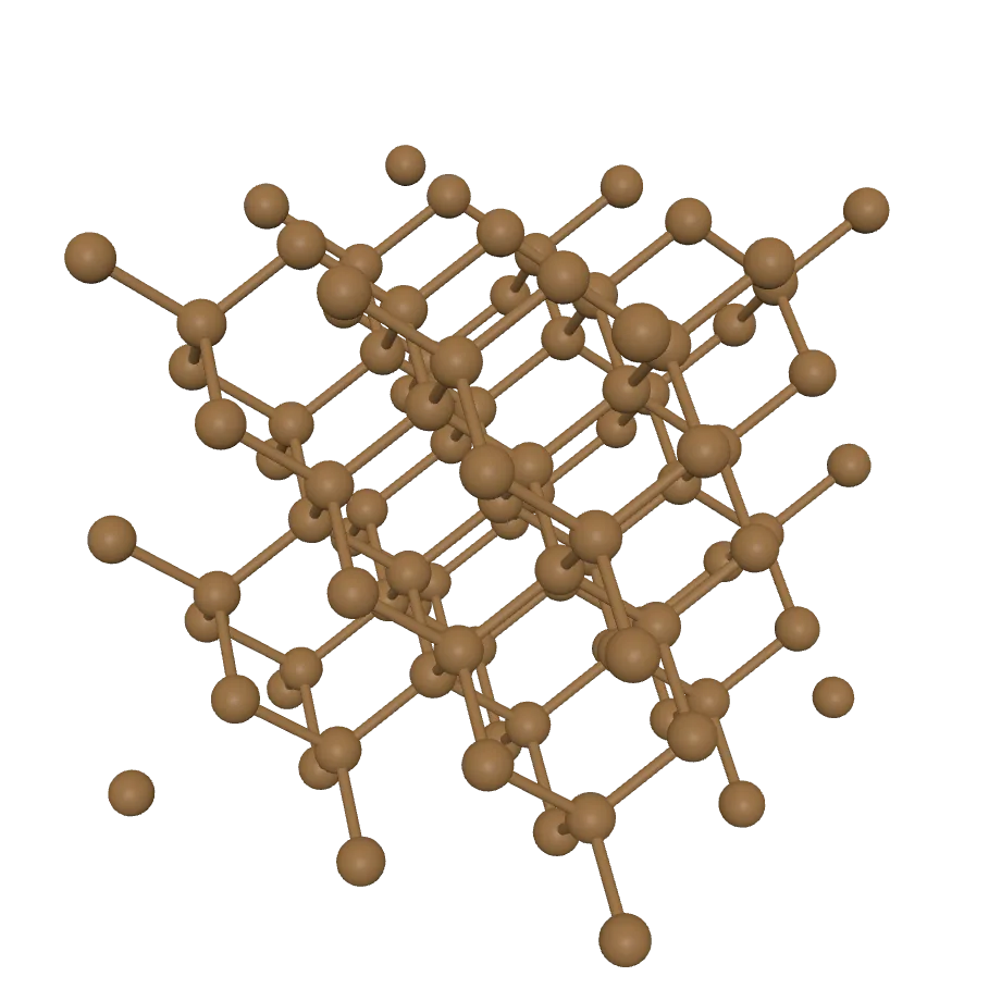
This browser can’t show the 3D model. The picture above is the same model.
A real silicon crystal, two repeating cubes each way: every silicon atom inside is bonded to four others, and the bonds run through the whole crystal in three dimensions.
One atom’s four neighborsEach atom sits at the center of a tetrahedron of four neighbors, 0.235 nm away, every two bonds 109.5° apart. Each bond is one pair of shared electrons, so all four outer electrons are held in bonds.
Drag to turn it. Tap a part, or a name below, to pick it out; tap it again to see the whole.
Silicon: COD 9011998, Hom, Kiszenick and Post (1975), Crystallography Open Database, CC0: www.crystallography.net/cod/9011998.html
The hole
The ambient temperature is the temperature of the surroundings. Above absolute zero (−273 °C), the atoms of a silicon crystal vibrate, and the higher the temperature the more strongly they vibrate. (The warmth you feel when you pick up a warm object is the effect of its vibrating atoms.)
Now and then, these vibrations shake an electron out of its bond. It is then free to move through the crystal: in the band picture, it has jumped into the conduction band. Its departure leaves a gap in the bond, a hole. The atom it left now has one electron too few, so the hole behaves like a positive charge, and it attracts and captures any free electron that comes near. An electron from a neighboring bond can also slip into it, which moves the hole one bond over.
Holes are the crucial difference between conductors and semiconductors. They let semiconductors do all kinds of things that conductors can’t.
At room temperature, thermal energy makes only a few holes and free electrons in silicon: about one bond in 10¹³ is broken. To increase the numbers of holes and free electrons, the crystal is doped (section 25.5).
Main ideas
A hole and a free electron each carry a charge of 1.6 × 10⁻¹⁹ C, of opposite signs. At any instant, inside a silicon crystal:
- heat is creating new pairs, a free electron and a hole each;
- elsewhere, pairs are recombining: a free electron falls into a hole, and both disappear;
- some free electrons and holes exist for a while, waiting to recombine.
The average time between a free electron’s creation and its recombination is its lifetime: from nanoseconds to milliseconds, depending on the crystal’s purity.
Intrinsic semiconductors
An intrinsic semiconductor is a pure one, with no other kind of atom in it: a silicon crystal made of silicon atoms only. At room temperature a silicon crystal is a poor conductor, almost an insulator, because thermal energy makes only a few free electrons and holes.
In an intrinsic semiconductor, the number of free electrons is:
Pick an answer to see why.
25.5 Doping a semiconductor
To make a semiconductor conduct better, we dope it: we add impurity atoms to the pure crystal, on purpose, to change how well it conducts. A doped semiconductor is called an extrinsic semiconductor. Only a tiny amount is added, often about one impurity atom per 10⁶ to 10⁸ silicon atoms, yet it can raise the conductivity of silicon thousands or millions of times.
Increasing the free electrons
How is the impurity put in? One way is to melt pure silicon (at 1414 °C), which breaks the covalent bonds and turns the solid into a liquid, add the impurity, and grow a new crystal from the melt. (Chips are also doped afterwards, by heating the silicon in a gas of the impurity, or firing impurity ions into its surface.)
To increase the number of free electrons, pentavalent atoms are added: atoms with five outer (valence) electrons, such as phosphorus, arsenic and antimony. They give, or donate, an extra electron to the crystal, so they are called donor impurities.
When the doped crystal cools and forms its solid structure again, each pentavalent atom takes a silicon atom’s place, surrounded by four silicon atoms. Four of its five outer electrons form bonds with the four neighbors, as a silicon atom’s would. The fifth has no bond to join. It is held only very weakly, by about 0.045 eV, so at room temperature, with eV, almost every such electron breaks free and becomes a free electron. The donor atom, having lost it, is a fixed positive ion.
So each donor atom in a silicon crystal gives one free electron, and the amount of impurity sets the conductivity: more donors, more free electrons, a better conductor. Silicon with only a little impurity (lightly doped) still has a high resistance; silicon with a lot (heavily doped) has a low one.
Increasing the number of holes
To make an excess of holes, a trivalent impurity is used, one whose atoms have only three valence electrons: boron, aluminium, gallium or indium.
A trivalent atom in the crystal is surrounded by four silicon atoms. It has only three outer electrons to share, so one of its four bonds is one electron short: there is a hole beside each trivalent atom. An electron from a neighboring bond easily moves into it (this takes only about 0.045 eV for boron), and the hole moves away through the crystal as a free hole, while the boron atom, now with an extra electron, becomes a fixed negative ion. A trivalent atom is called an acceptor atom because each hole it gives can accept an electron.
Two types of extrinsic semiconductor
Doping can give a semiconductor either more free electrons than holes, or more holes than free electrons, so doped semiconductors come in two types.
n-type semiconductor. Silicon doped with a pentavalent impurity is an n-type semiconductor, n standing for negative. The free electrons outnumber the holes, so the free electrons are the majority carriers and the holes the minority carriers.
p-type semiconductor. Silicon doped with a trivalent impurity is a p-type semiconductor, p standing for positive. The holes outnumber the free electrons, so the holes are the majority carriers and the free electrons the minority carriers.
In each crystal, the applied voltage moves the free electrons to the left, towards the positive terminal, and the holes to the right.
- In n-type, the many free electrons reach the left end of the crystal, enter the wire and flow on to the positive terminal of the battery. When one of the few holes reaches the right end, a free electron from the wire there enters the crystal and recombines with it.
- In p-type, the many holes reach the right end, where each recombines with a free electron entering from the wire. Meanwhile the few free electrons inside the crystal drift from right to left; because there are so few of these minority carriers, they have almost no effect on the current.
In both, the current in the wires is carried by electrons, and the conventional current flows the same way: out of the battery’s positive terminal and round the circuit.
Silicon is doped with gallium. The result is:
Pick an answer to see why.
25.6 The p–n junction
Most uses of semiconductors join p-type and n-type material in one crystal. The boundary between them is a p–n junction, and it behaves in a way neither material does alone.
The depletion layer. At the moment the junction forms, the n side has many free electrons and the p side many holes. Free electrons near the junction diffuse across it into the p side, and holes into the n side, each spreading from where there are many to where there are few, and they recombine. This leaves a thin layer on each side of the junction, about a micrometer thick, with almost no free carriers: the depletion layer. It is not neutral, though: on the n side it holds the positive donor ions the electrons left behind, and on the p side the negative acceptor ions.
The barrier potential. These fixed charges make an electric field across the depletion layer, pointing from the n side to the p side, which pushes back any more electrons trying to cross. Diffusion soon stops. The potential difference across the depletion layer is the barrier potential: about 0.7 V for silicon and 0.3 V for germanium.
Bias. A junction with a voltage across it is said to be biased.
- Forward bias: p side to the positive terminal. The supply’s voltage works against the barrier, the depletion layer narrows, and once the supply is above the barrier potential, electrons and holes cross freely: a large current flows.
- Reverse bias: p side to the negative terminal. The supply adds to the barrier, the depletion layer widens, and only a tiny current of minority carriers flows, usually less than a microampere.
So a p–n junction, a diode, lets current through in one direction only.
Rectifiers and transformers. The mains supply in Nepal is alternating current, 230 V at 50 Hz, but phones, laptops and LEDs need direct current at a few volts. A charger does two jobs. A transformer changes the size of an alternating voltage, down from 230 V to a few volts (it works only with a.c.). A rectifier, made of diodes, then converts the a.c. to d.c., because each diode passes current only one way: one diode gives half-wave rectification, and four in a bridge use both halves of each wave. A capacitor smooths what is left.
Exercise
Choose the correct option
- The barrier potential difference is the potential difference across:
Pick an answer to see why.
- A transformer is a device to:
Pick an answer to see why.
- a.c. is converted to d.c. by a:
Pick an answer to see why.
- When pure germanium is doped with a trivalent impurity like aluminium, conduction is due to:
Pick an answer to see why.
- If germanium is doped with a donor impurity, the donor atoms should be:
Pick an answer to see why.
- A sample of n-type silicon:
Pick an answer to see why.
- When arsenic is added as an impurity to silicon, the resulting material is:
Pick an answer to see why.
- Three semiconductors are arranged in increasing order of their energy gaps. The correct arrangement is:
Pick an answer to see why.
- A p-type semiconductor is:
Pick an answer to see why.
- The current through a p–n junction is negligible when the junction is:
Pick an answer to see why.
- Silicon is a semiconductor. On adding a small quantity of arsenic to it, its conductivity:
Pick an answer to see why.
- Indium is mixed into a silicon specimen, on average one indium atom per 10⁸ silicon atoms. If the number density of atoms in the silicon is 5 × 10²⁸ atoms/m³, the number and nature of the impurity atoms per cubic meter are:
Pick an answer to see why.
Answer these questions
On the basis of the band theory of solids, how would you distinguish between a conductor and a semiconductor?
Answer
How is a p-type semiconductor formed? Explain.
Answer
When p-type and n-type materials are joined, a depletion layer forms at the junction. Why?
Answer
How does the conductivity of a semiconductor vary with temperature? Explain.
Answer
The conductivity of an intrinsic semiconductor is low. Why?
Answer
Why is a semiconductor virtually an insulator at room temperature?
Answer
What do you mean by doping?
Answer
What do you mean by the forbidden energy gap?
Answer
What is an extrinsic semiconductor? Explain the formation of the potential barrier and the depletion layer at a p–n junction.
Answer
Printable PDFs
- The unit as a book (A5) 22 pages Answers as an A4 booklet, 6 sheets
- Study notes 3 pages
- Worksheet 5 pages Answer key
- Harder practice questions 2 pages Answer key
Quiz yourself: Matter, Atoms and Reactions, Grades 5–12 →
Practice every question in the book, and keep track of the ones you miss →
A companion to your textbook, not a replacement for it: study from the book your school uses, and where the two differ, follow your teacher. Found a mistake? Please tell us.